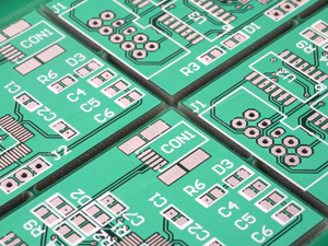
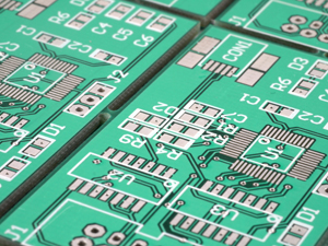
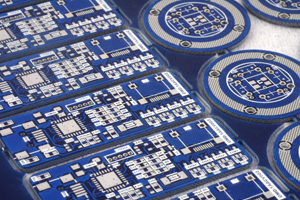
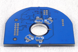
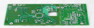
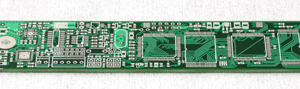
Product samples and specifications
|
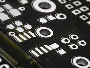
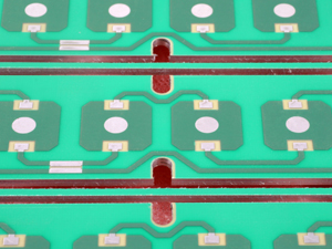
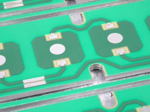
Specifications of printed wiring boards available for ordering:
- Minimum track width at single- and double-sided boards is 0.2 mm; minimum track width at multilayer boards is 0.25 mm
- Minimum track to track insulation spacing is 0.25 mm
- Minimum track to pad and pad to pad insulation spacing is 0.25 mm
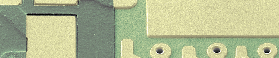
- Minimum finished hole diameter is 0.3 mm
- Rigid, single-sided, double-sided and multilayer constructions up to 8 layers
- FR4 epoxy-fiberglass laminates in different thicknesses (0.2; 0.25; 0.4; 0.5; 0.8; 1.0; 1.2; 1.55; 2.0; 2.5 mm)
- Bright electroplated tin, or selective chemical silver solder pad surface finish
- Photosensitive solder mask coating and legend
- CNC contour milling in custom sizes, or in panelised design with tabs to allow breaking appart
- Ordering lead time is between 1 or 15 working days; in the case of multilayer boards at least 3 working days
The printed wiring boards can be designed with a computer and CAD systems. Please make the necessary documentation for ordering with CAD systems by taking the followings into consideration:
- For the plotting of films, RS274X format Gerber (extended Gerber) files are necessary for each layer. If the CAD programme is an older one, it can occur that it recognises only RS274D format. In this case aperture list should be attached to the Gerber files
- We require the drilling programmes in EXCELLON or ASCII format, possibly with INCH 2.4 ABSOLUT TRAILING settings, and the diameters of drilling tools in the file indicated with standard signs (e.g. T1C0.040, T2C0.124)
- Please do not modify the syntactic format of the drilling programme that were made by the CAD system; if comments are required, please write them in the beginning of the file in a separate line in brackets. Please provide the diameters of drilling tools in the same unit which is also given for the coordinates
- The diameter of the holes in the drilling programme equals with the diameter of the drilling tools. The finished hole size will be cca. 0.1 mm less in the case of printed wiring boards with plated through-holes. If the hole diameters given in the file equal with the finished size, please indicate it in the ordering form or in the beginning of the drilling file
- In the case of multilayer boards, the diameter of the innerlayer annular rings should be with 50 mils (1.27 mm) larger than the diameter of the holes at the power and ground layers
- If the pattern contains copper pour (e.g. ground plane) then the insulation spacing should be at least 20 mils (0.5 mm) between the pattern and the copper pour; crosshatch fill style is more preferred than continuous, full filling of copper pour
The finished products can be taken over at address 1111 Budapest, Egry JĂ³zsef u. 18., Building V1 by heading down half floor from the hall (V1C), and by pushing button 1 of the entryphone at the grey door on weekdays between 08:00 and 16:30.
|